| Part #: | OP103 |
| Description: | FPGA Mezzanine Card with 8x MCIO PCIe Gen4 connector and redrivers |
| Vadj: | 1.2V-3.3V |
| Price: | USD $595.00 |
| HTS: | 8473.30.1180 |
| Sched B: | 8473.30.0002 |
| HS Code: | 8473.30.00 |
| ECCN: | EAR99 |
| Origin: | Canada (CA) |
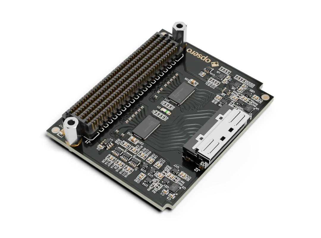
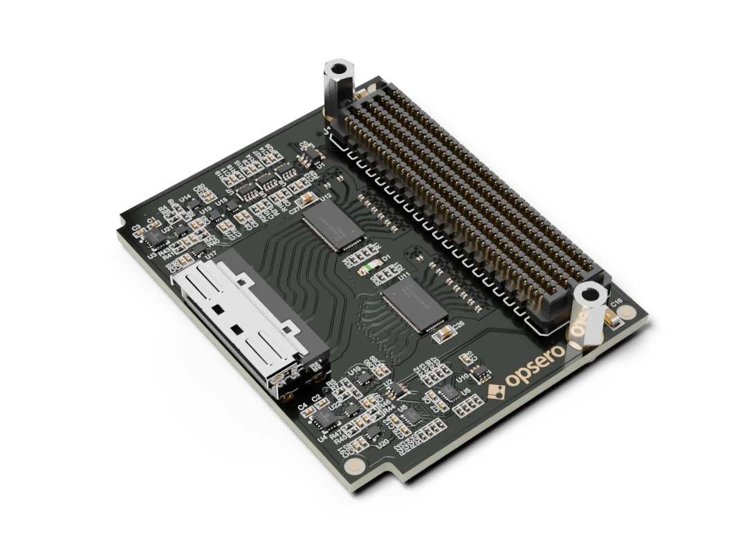
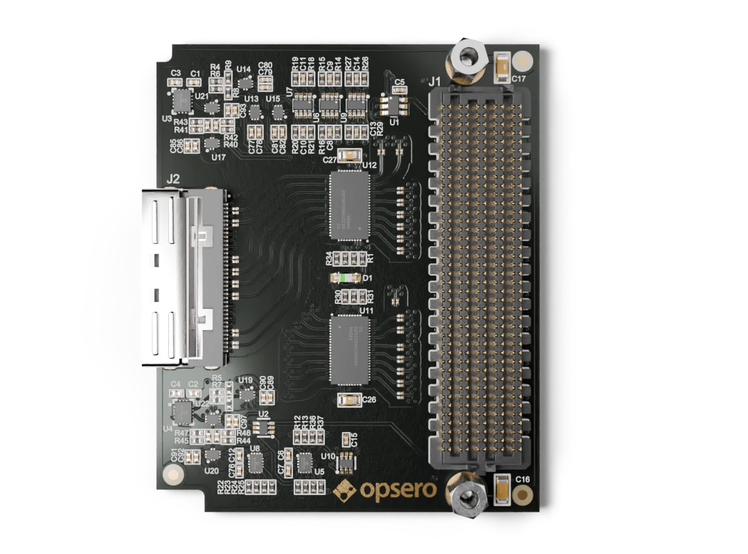
MCIO PCIe FMC
Where to buy
| Opsero Direct: (Ships from Canada) |
6 pcs in stock (can ship immediately) |
| Digi-Key: (Ships from USA) | Buy it from Digi-Key |
Description
The MCIO PCIe FMC is an FPGA Mezzanine Card designed to bring high-speed MCIO connectivity to FPGA and adaptive SoC development platforms. It supports cabled PCIe Gen4 connections with up to 8 lanes or dual 4-lane (2x4) configurations, enabling direct interface with high-performance devices such as NVMe SSDs, GPUs, custom accelerators and other FPGA boards. The board integrates two TI DS320PR810 PCIe redrivers to compensate for signal loss, ensuring reliable signal integrity over MCIO cables and adapters. For more detailed information on the MCIO PCIe FMC, including datasheets, schematics and example designs, please see the datasheet.
- 8-lane MCIO PCIe connector
- Supports both host and device mode determined by a logic signal
- Supports up to PCIe Gen4
- 2x PCIe redrivers TI DS320PR810
- HPC FMC compliant with VITA 57.1
- Supports a wide range of I/O voltages (VADJ): 1.2V-3.3V
- Reference designs for multiple FPGA and MPSoC development boards
- Straightforward tech support
Frequently asked questions
What are the supported PCIe link speeds?
This product supports up to PCIe Gen4 (16Gbps per lane) on all 8 lanes.
What FPGA I/O voltages (VADJ) are supported by MCIO PCIe FMC?
The MCIO PCIe FMC was designed with level translators to enable it to support any VADJ voltage in the range of 1.2VDC to 3.3VDC.
Is the MCIO PCIe FMC compatible with my FPGA board?
In general terms, the FPGA development board needs to have gigabit transceivers to use the MCIO PCIe FMC, and those transceivers must be connected to the DP0-7 pins of the FMC connector. It also needs to be able to supply a VADJ voltage between 1.2VDC to 3.3VDC. Please visit the product website for a list of compatible FPGA boards and detailed compatibility requirements.
Do I need any purchased IP to use the MCIO PCIe FMC?
For generic applications: This product can be used with free IP cores such as Aurora for generic applications where we require high throughput connectivity between two FPGA devices. In these applications, you do not need any paid IP.
For PCIe applications: The minimum requirement for interfacing an FPGA with a PCIe device is a PCIe IP core, which tend to be paid cores. However, these days many FPGA development boards have an FPGA with integrated PCIe block. If your FPGA board has an integrated PCIe block, and the corresponding gigabit transceivers are routed to the FMC connector, you will not need any purchased IP to use the MCIO PCIe FMC. The reference designs rely on the Xilinx PCIe integrated block and they allow a U.2 NVMe SSD to be accessed in PetaLinux. In that use case, the NVMe protocol is handled by the operating system, or more specifically by the embedded microprocessor. If you have an application where the NVMe protocol must be handled in the FPGA fabric, you may require purchased IP.